
The Monkeyprint DLP printer board requires you to make your own PCB. This can be intimidating if you’ve never done it before. But don’t be afraid! I show you how it’s done…
In this tutorial you will learn how to etch a PCB using the photo resist method. At the end you will be holding your own Monkeyprint DLP printer board in your hands. But first things first:
Warning & disclaimer
You will be working with potentially hazardous chemicals. When handling these chemicals comply to the following rules:
- Use gloves.
- Wear a lab coat.
- Use safety goggles.
- Don’t eat, don’t drink.
- Do not store chemicals in food containers. Use chemical bottles (you can get them at your local drug store) and label them properly.
- Do not store chemicals in your kitchen or any other place that might be accessed by an unsuspecting person.
Disclaimer: This is a do-it-youself guide and you follow the instructions at your own risk. I cannot be held liable for any effects your actions might have, including injury or damage.
Overview
There are several ways of making a PCB from a copper plated board. All of them involve masking the traces and pads by some sort of etch resist and then etching away the unmasked parts of the copper. The difference lies in how the etch resist comes onto the board. You can paint the layout onto the board using etch resistant markers, you can use the toner transfer method or you can use boards that come with a photo active etch resist and need to be exposed and developed before etching.
The last — the photo resist method — offers the highest level of quality — and that is why we will use it here. Additionally, it’s very similar to printing with a DLP printer 🙂
This method includes the following steps:
- Get the layout transferred onto an exposure mask.
- Expose the board using the mask and develop it.
- Etch the board.
- Tin coat and drill the board.
Step 0: Make an exposure mask
First of all, we need to make a mask that contains the layout of the Monkeyprint DLP printer board. Traces and pads need to be black and everything else transparent. You will find the layout as a pdf file in DIN A4 format in the hardware folder of your Monkeyprint directory. If you don’t have it already, check it out on my Github.
The best way to make the mask is to have your local print shop expose the layout onto transparent film. This results in a superior quality mask as the resolution is very high. The cost is about 7 € in the print shop of my choice for a DIN A4 film.

As an alternative, you can print onto transparent foil (overhead slides) using a laser printer. Make sure to use A4 format and 100% scaling!
Step 1: Cut a piece of PCB to size
Equipment:
- A PCB with photo resist coating. I use Bungard PCBs as they work really well. Pay attention to the best before date: PCBs that are too old might not work anymore as the etch resist degrades over time.
- A Jigsaw, pen and ruler.
- Sanding paper, grit 240–320.
Instructions:
Mark a rectangular area of 69 x 60 mm on the PCBs cover foil. This is larger than the layout by 2 mm on all sides, which can be advantageous as the etch resist will sometimes be damaged on the edges. Then, cut out the marked area.
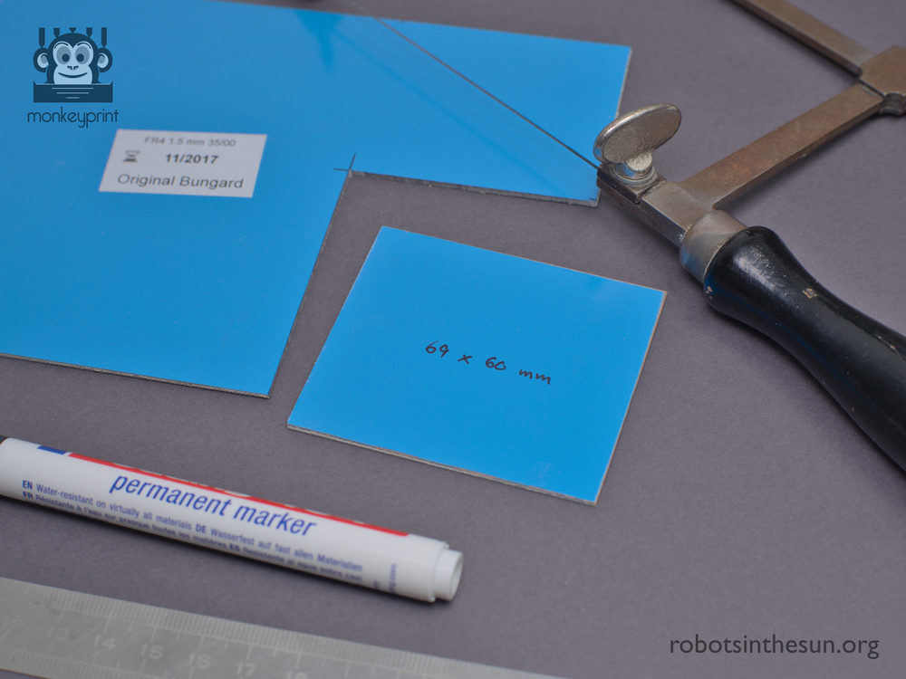
I cut the PCB with a jigsaw. Make sure to deburr the edges, especially on the copper plated side as the exposure mask needs to lay down really flat onto the board later on.
Step 2: Expose and develop the PCB
In the next step you are exposing and developing the PCB. The exposure will be done using UV light and the exposure mask. After the exposure the board needs to be developed. This will wash away the photo resist where it has been exposed to the UV light and leave the resist only where the layout mask was black.
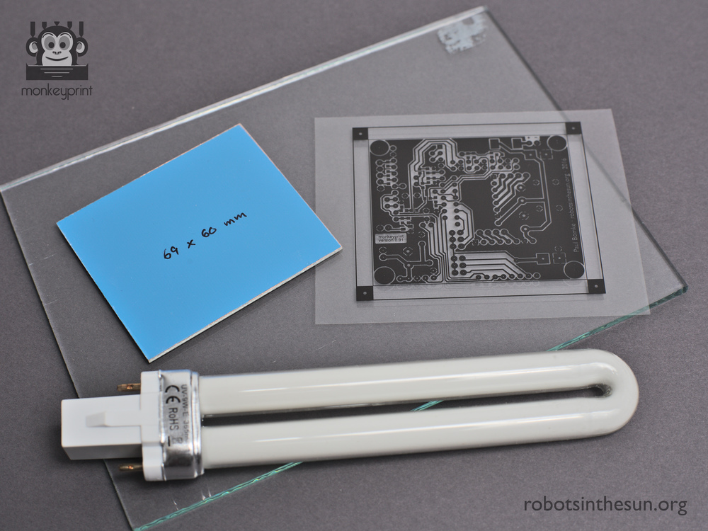
Equipment:
- A cheap nail polish curing lamp. You can get it on eBay for about 15 €. You only need to install two of the four UV lamps provided.
- A glass plate of about 100 x 100 mm. Clean it with some ethanol or window cleaning detergent.
- The exposure mask.
- An etch resistant flat (glass) basin.
- Developing solution. For Bungard PCBs use 20 grams of NaOH in 1 liter of water. If you use different material refer to the data sheet or manual.
 Danger! NaOH is corrosive and might lead to serious injury on skin or eye contact. Wear gloves and safety goggles, do not eat or drink during the process.
Instructions:
Before you start, pour some developing solution into the basin and heat it up to about 50° C. Also make sure your UV lamp is plugged in and operational and your glass plate and exposure mask is at hand.
Then, follow the steps below:


Result:
Congratulations! You now have completed the most critical step of the process. The board is now insensitive to light and ready to be etched. If you do not want to do the etching right now, cover it with the sticky tape again to protect the etch resist.

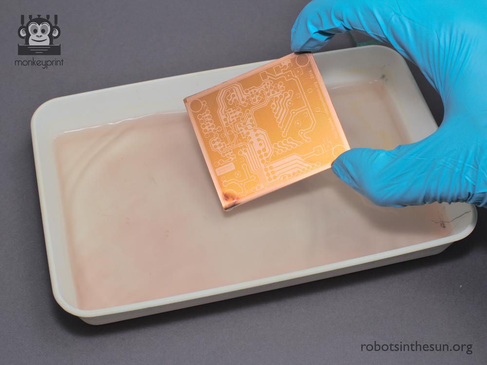
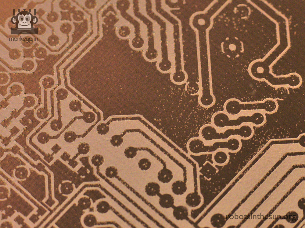
Step 3: Etch the PCB
During this step you will etch away the copper where the etch resist has been removed from the board in the previous step.
Equipment:
- The exposed and developed board.
- An etch resistant flat basin and etch resistant pliers.
- Etching solution. Some use ferric oxide, I use sodium persulfate (Na2S2O8). You can buy it in a drug store or at your electronics supplier. Dissolve 250 grams in one liter of water.
Danger! Na2S2O8 is corrosive and might lead to serious injury on skin or eye contact. Wear gloves and safety goggles, do not eat or drink during the process.
Na2S2O8 will gradually release oxygen during storage. Use a bottle with an overpressure valve, otherwise your container might burst.
First, heat up your etching solution to about 50° C. I do this in a water basin on a regular stove as I don’t have a lab stove with regulated temperature. Then, follow these steps:


Step 5: (optional) Tin coating
This step is optional. Tin coating the board prevents corrosion of the copper and makes the soldering a little easier. It also looks better (which is the main reason why I like it).
Equipment needed:
– Soldering iron.
– Solder. I use Sn62Pb36Cu2 with a flux core.
– Solder wick. Apply some flux onto the wick for better results.


There are certainly more elegant ways of tin coating your board like tin baths, so if you want to use a different method or skip this step all together, I won’t blame you 🙂
Step 6: Drilling and trimming
The last step is very easy and straight-forward.
Equipment:
- Hand tool.
- 0.8 and 1.0 mm drill.
- Jigsaw and sanding paper.
Instructions:
- Place the board onto a flat piece of wood and drill all holes with a diameter of 0.8 mm.
- Then, drill the holes for the angled connectors, the straight connectors and the step down converter with 1.0 mm.
- Drill the mounting holes with 3.5 mm.
- Cut off the offset edges up to the thin line around the layout. You can use the jigsaw again to do this. Make sure to sand the etches to get a smooth finish.

What’s next?
You now hold your first, self-made Monkeyprint board in your hands. Congratulations!
In the upcoming part of this tutorial I will show you how to solder the components and connect your PC and the other peripherals.
If you encounter any problems, have questions or remarks, please comment below!
Good luck and best wishes,
Paul
Hello Paul, I loved the Monkeyprint DLP, I plan to use it on the machine I’m going to build, but I’d like to know a few things:
Did you give up on PCB and firmware? Not available in github.
Would this pcb not work on an Orange Pi? which is much cheaper.
I have a dlp Chinese printer and they use an Orange pi lite with a proprietary pcb and a proper slicer as well. (it’s Micromake L2)
I do not want to stick with the nanodlp solution, and I liked the solution.
Thank you